About This Project
For decades we’ve been shrinking our electronics to make them cheaper, faster, and more efficient. Recently discovered two-dimensional (2D) semiconductors that are only 3 atoms thick, flexible, and strongly absorb and emit light stand as the ultimate limit of this endeavor. With these, we aim to make a scalable and efficient, all-2D LED and solar cell. This will enable a future filled with transparent and flexible displays and solar panels.Ask the Scientists
Join The DiscussionWhat is the context of this research?
A family of light-active, two-dimensional (2D) semiconductors has been identified and intensely studied in recent years. These materials are only three atoms thick but exist in large area sheets. They do not break down in air or water and are thus safe in most applications.
Using the 2D semiconductor tungsten diselenide, we recently demonstrated how it can function as a 2D LED, the thinnest LED possible! If run backward, this device also works as a solar cell since the fundamental component, the p-n junction, is the same.
This design used thick metal layers and only produced light at a small region. The next step is to incorporate graphene, a conductive 2D layer of carbon atoms, to enable an all-2D design that emits light across the entire device area and is scalable and efficient.
What is the significance of this project?
This work can have significant impact on the cost of production of lighting displays and solar panels because the amount of material needed is greatly reduced when using 2D materials.
2D materials are mostly transparent and extremely flexible, so LEDs and solar cells made from them can be hidden in a window, in a contact lens, or in a flexible mobile device. One can imagine remarkable impacts on augmented reality and sustainable energy technologies.
We will enable these impacts by figuring out how exactly to construct such a device as well as study the physics of its performance. To this end, we will collaborate with another lab that specializes in making high performance 2D electronic devices and use our expertise in semiconductor optics measurements to understand and improve the design.
What are the goals of the project?
- Investigate which 2D semiconductors can be combined to form the p-n junction for LED and solar cell functionality.
- Learn new 2D material stacking and device fabrication techniques from collaborators so graphene electrodes can be incorporated, resulting in an all-2D device.
- Develop a simple and scalable procedure to produce the vertical stack of 2D materials that functions as both an LED and a solar cell.
- Study the performance and physics of this device with our state-of-the-art cameras and measurement techniques and use this knowledge to improve upon the design.
Budget
We believe exciting technological ramifications would be best supported by immediate public funding. Your support will enable us to begin this important work and ensure that the results are not tied to corporate sponsors or hinged on uncertain federal funds.
Specifically, key components in the proposed work cannot happen without funding.
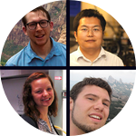
Leading the project is PhD student Jason Ross, creator of the thinnest LED. He will learn new graphene electrode and clean 2D stacking techniques by visiting Professor James Hone’s group at Columbia University. Funds for travel and living expenses are necessary to make this collaboration possible.
This project also requires significant materials processing and device fabrication procedures using state-of-the-art instruments in the Washington Nanofabrication Facility, a pay-by-the-hour clean room user facility.
Exceeding the necessary budget and improving project
success:
$1500 extra
We have recruited a very talented undergraduate student, Marie Scott, who has become the lab expert in 2D materials production and stacking techniques. Making a single device properly can sometimes take months and thus funding Marie for full-time work in the lab while she completes coursework will significantly boost the project's success.
$1000 more
will buy us a motorized micromanipulator controller allowing faster, more accurate layer stacking procedures.
Meet the Team


Team Bio
Jason RossJason has always been passionate about applying nanoscience to real world applications. With his recent breakthroughs in tuning 2D excitons and making the thinnest LED, he is becoming an important researcher in the field, both in understanding these new materials and making useful technologies from them. Outside lab he enjoys hiking, android app development, and seeing live music.
Dr. Xiaodong Xu
Professor Xu has emerged as a leader in the field of low-dimensional quantum systems for new electronic and photonic technologies, continually adding indispensable knowledge, especially in 2D material physics and applications.
Pasqual Rivera
Pasqual is a PhD student who's recently made strides in understanding how two 2D semiconductors interact, forming a heterojunction. This will be key to the all-2D LED.
Marie Scott
Marie is our most talented undergraduate researcher with a talent and passion for assembling 2D devices rivaled by none.
Xiaodong Xu
I am a condensed matter experimentlist at University of Washington. My current research focus on understanding the fundamental properties of new low dimensional quantum materials for novel device technologies. Please check out my website for more information http://depts.washington.edu/xulab/.
Lab Notes
Nothing posted yet.
Press and Media
Our recent article “Electrically tunable excitonic light-emitting diodes based on monolayer WSe2 p-n junctions.” In Nature Nanotechnology received extensive media coverage this last March.
Additional Information

Atomic arrangement of atoms in our 2D semiconductors and a microscope image. Despite being only 3 atoms thick, you can see a single layer in a conventional microscope because of how strongly it interacts with light. It's amazing!
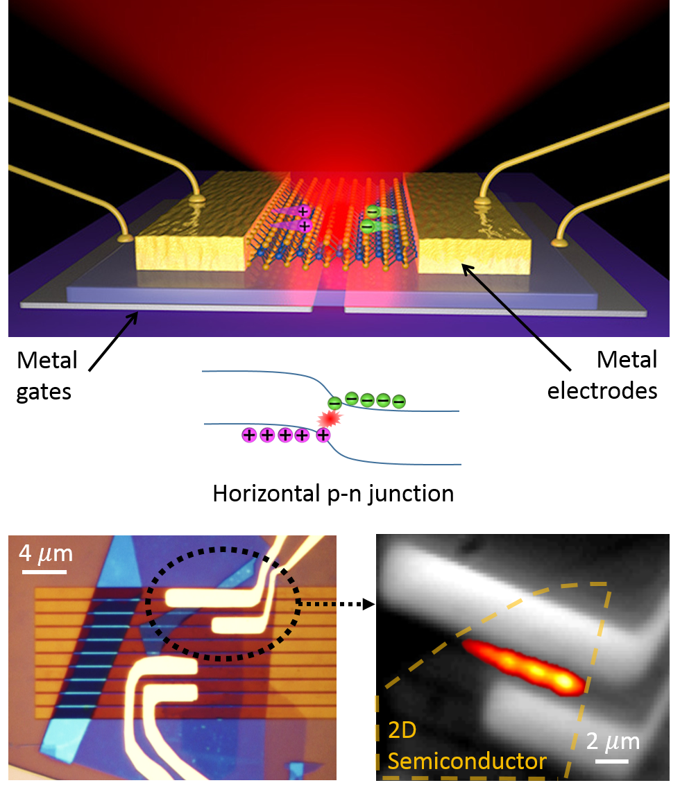
With a single 2D layer, our old LED design used thick metal gates and electrodes to establish and drive a horizontal p-n junction, the fundamental component of LEDs and solar cells. Top: cartoon of device. Bottom left: microscope image of two devices. Bottom right: false colored measurement of actual light emission.
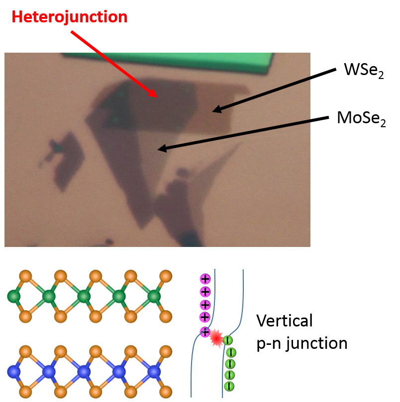
Stacking two different 2D semiconductor materials forms a natural p-n junction due to the different energy levels in each material. This makes a vertical p-n junction at the entire area of overlap.

Using graphene electrodes and the naturally formed vertical p-n junction, we will make an efficient large area 2D LED and solar cell.
Project Backers
- 11Backers
- 18%Funded
- $800Total Donations
- $72.73Average Donation